
The global semiconductor landscape is witnessing a strategic shift in manufacturing philosophy as the world’s leading foundry seeks to maintain technical momentum without the immediate adoption of prohibitively expensive hardware.
This approach is designed to produce smaller and more efficient processors using its current fleet of extreme ultraviolet machines. By bypassing the immediate need for the latest generation of lithography tools, the firm aims to balance aggressive scaling with cost efficiency for its diverse client base.
An equity research specialist at Finio24 notes that these evolving conditions represent a focused attempt to extend the economic viability of current production environments. For institutional investors monitoring the financial trajectory of the technology sector, this manufacturing strategy offers a buffer against rising capital expenditure.
Strategic Scaling And Lithography Cost Management
During a recent industry event in Santa Clara, the foundry giant introduced two pivotal technological advancements: the A13 process and the N2U variant. The A13 technology is slated for high volume production in 2029 and is specifically engineered to meet the massive compute requirements of future artificial intelligence frameworks.
Meanwhile, the N2U process offers a more cost-effective alternative for consumer electronics such as smartphones and laptops, while still providing significant performance upgrades. A key takeaway for market participants is the decision to leverage existing extreme-ultraviolet (EUV) systems rather than transitioning to the newest “high NA” EUV machines.
These newer units carry a price tag of roughly $400 million each, which is approximately double the cost of the currently utilized equipment. Senior leadership at the firm noted that their research and development teams have successfully maximized the capabilities of existing technology to set a competitive scaling roadmap.
This move is seen as a major strength, allowing the company to maintain institutional-grade productivity without passing massive capital expenditure increases onto customers.
Multi-Die Packaging and The Evolution Of Moore’s Law
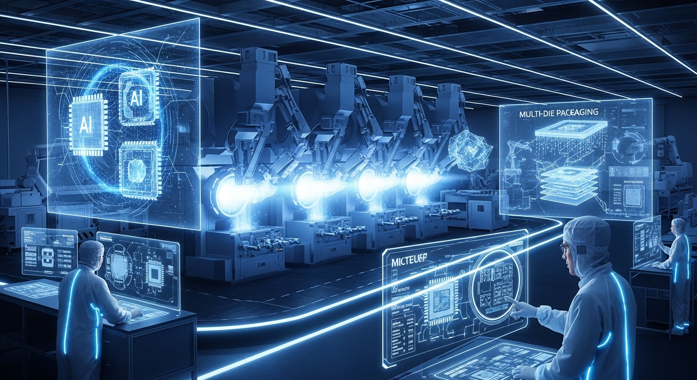
While the gains from traditional transistor shrinking are becoming more incremental, the industry is increasingly looking toward advanced packaging techniques to drive performance. The foundry revealed that by 2028, it expects to have the capability to integrate 10 large computing chips and 20 stacks of high-bandwidth memory within a single package.
This represents a significant escalation from current high-end AI offerings, which typically feature two computing dies and eight memory stacks. This transition from monolithic, single-die designs to complex multi-die configurations is effectively redefining the parameters of Moore’s Law.
The future expectations for the sector are now tied to the success of these packaging innovations. By combining heterogeneous dies into a unified structure, manufacturers can bypass some of the physical constraints of individual silicon wafers.
Thermal Management And Structural Integrity Challenges
As chip packages become larger and more complex, they encounter significant thermal and mechanical hurdles. The various materials used in multi-die packaging expand at different rates when exposed to the intense heat generated during high-speed AI processing.
This differential expansion can lead to structural failures, such as bending or cracking, which have been documented in recent high-performance processor designs. Designing systems that can dissipate heat efficiently while maintaining structural stability is now a primary focus for the firm’s engineering teams.
The strategic direction involves developing new materials and cooling solutions that can withstand the rigors of modern enterprise computing. For institutional holders, the financial trajectory of the company will depend on its ability to solve these packaging bottlenecks as the demand for larger, more powerful AI clusters continues to rise.
The longer-term positioning of the foundry remains robust, as it serves the world’s largest technology enterprises, including providers of major search engines and mobile operating systems. These clients are increasingly dependent on the foundry’s ability to deliver specialized silicon that can handle massive algorithmic workloads without compromising on energy efficiency.
AI Chip Innovation, Efficiency, and Strategic Direction
In conclusion, the decision to optimize existing manufacturing assets while doubling down on advanced packaging reflects a pragmatic approach to the current semiconductor cycle. By avoiding the immediate financial burden of the newest lithography tools, the company is positioning itself to offer competitive pricing during a period of high capital intensity.
Monitoring the financial trajectory of the silicon market will provide essential insights into how manufacturing leaders navigate the transition to post-monolithic architectures. The evolving conditions of the global hardware market favor firms that can demonstrate both technical ingenuity and fiscal discipline.
Maintaining institutional-grade productivity remains the ultimate objective as the industry moves toward the 2029 production horizon. Ultimately, the future expectations for the technology sector are centered on the integration of massive compute and memory resources.
The strategic direction is clear: leverage packaging complexity to overcome the limitations of traditional scaling. As the digital economy continues to prioritize artificial intelligence infrastructure, the ability to deliver high-performance silicon at scale will remain the most critical factor in global technological leadership.
